A key slid into the lock, turned halfway. Sam Altman and Broadcom CEO Hock Tan stood side by side on stage, holding a 300mm silicon wafer imprinted with the chip named “Jalapeño.” The shutter clicks from the audience came down like a rainstorm. On June 24, 2026, OpenAI finally played its first hardware card.
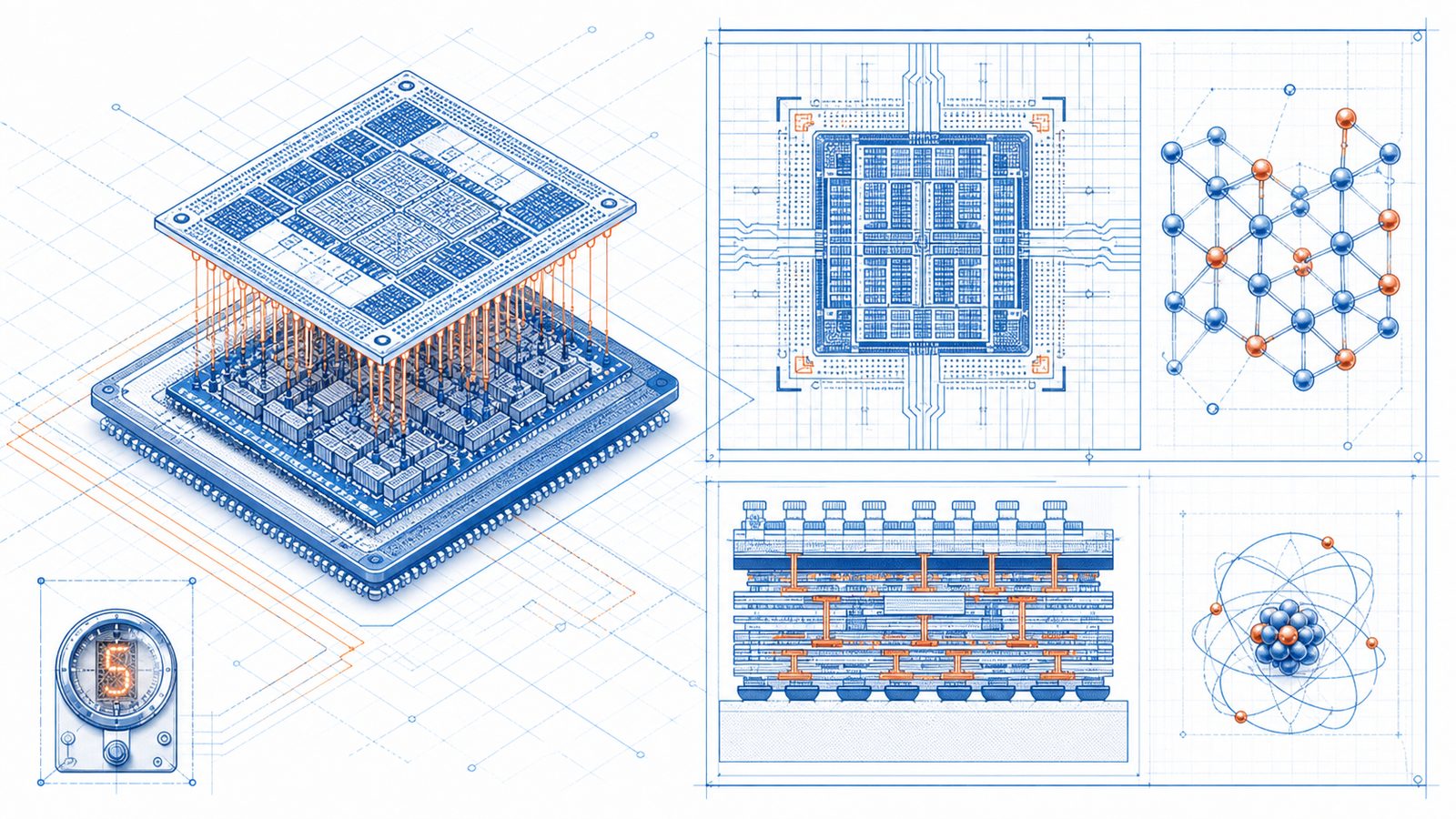
From publicly available information, Jalapeño is a dedicated inference ASIC, co-developed by OpenAI and Broadcom, manufactured on TSMC’s 3nm process, equipped with 8 HBM stacks, with die area approaching the reticle limit. The chip uses a systolic array architecture — the wafer photo reveals highly repetitive columnar floorplan patterns, similar to features observed in Broadcom’s previous physical design work for Google TPUs. The first engineering samples are already running GPT-5.3-Codex-Spark and have hit target frequency and power targets.
One sentence in OpenAI’s official statement triggered collective pushback from the chip community: “From design to production, it only took nine months.” Bloomberg’s coverage added Hock Tan’s claim — that compared to typical GPU inference solutions, Jalapeño can save approximately 50% in costs. Put these two data points together, and you get the core narrative of this launch: fast, and cheap.
But what exactly is this “9 months” measuring? In the HN discussion, a user “zgao” who claimed to be a chip company CEO offered an engineer’s perspective. If “design” means RTL freeze (front-end logic design frozen), and “production” means tapeout (submission to the fab for manufacturing), then 9 months for a large, complex chip on a 3nm process is “a fairly routine, even not particularly impressive timeline.” But if it means from “concept stage” — no architecture block diagram, not a single line of RTL written — to tapeout in just 9 months, that would be truly astonishing. And since OpenAI didn’t specify the exact milestones for start and end, “the truth is probably somewhere in between.”
Another user, “sharkjacobs,” was more direct: if AI models really played such a big role in chip design, would OpenAI just vaguely mention “our models accelerated the design and optimization process”? That sounds about as meaningful as “Microsoft Office accelerated our development” — filler for a slide deck. I tend to think this statement lies somewhere between fact and marketing. Hardware description languages (HDLs) like Verilog and SystemVerilog do have some coverage in LLM training corpora, and automated testbench generation is already a direction being explored in the industry. OpenAI has indeed hired for several chip design AI positions in recent months. But to claim it has formed a complete toolchain comparable to Google DeepMind’s AlphaChip — there is no public evidence of that yet.
This touches on a critical division of labor in the chip industry: front-end design and back-end implementation. Front-end is architecture definition and RTL writing — this was likely led by OpenAI’s hardware team, headed by Richard Ho, who was previously the hardware lead for Google’s TPU project and had worked with Broadcom during the TPU era. Back-end is the physical implementation of turning RTL into GDS (think of it as the chip’s layer-by-layer “Photoshop file”), plus subsequent supply chain management, packaging, and testing — and Broadcom is an absolute veteran at this. Someone put it harshly but accurately: “OpenAI did the architecture definition, Broadcom did everything else.”
If you understand this division of labor, whether “9 months” is reasonable depends on when you start the clock. From RTL freeze to tapeout, with Broadcom’s existing IP library and mature design flow, 9 months is a normal timeline. From concept design to tapeout, 9 months is nearly impossible — chip design is not software iteration; silicon has zero tolerance for error.
Now let’s look at technical details. Jalapeño is positioned purely for inference, not training. This choice has clear economic logic: training is a one-time cost, inference is an ongoing cost. The massive volume of inference requests OpenAI processes daily through ChatGPT, Codex, API, and other product lines is the real beast eating into profits. Moving inference off Nvidia GPUs, even if it only saves 30-50%, translates to billions of dollars in annual bill differences at scale.
Architecturally, Jalapeño uses a hybrid design of systolic arrays + fixed-function hardware, optimized specifically for forward propagation of Transformer-type models. This shares design philosophy similarities with Google’s TPU v1 — back then, the TPU v1 was also a pure inference chip, 92 TOPS@INT8, consuming only 40W, blowing contemporary GPUs out of the water in inference efficiency by orders of magnitude. But Google spent a full decade iterating TPU to its eighth generation, covering the complete workflow from inference to training. OpenAI has only just taken its first step.
How should we view this chip’s position in the competitive landscape? From an industry trend perspective, AI companies building their own chips has shifted from an option to a timeline question. Google TPU is already at gen 7/8, AWS has Trainium2 and Inferentia2, Meta’s MTIA series is advancing to 2nm in partnership with Broadcom. Anthropic is also exploring its own chip path, with using AWS Trainium to train Claude already being public information. The driving force behind this trend is clear: when your model architecture, operator combinations, and batching patterns are all internal knowledge, general-purpose GPUs have massive transistor counts powering features you don’t need.
But there’s a risk that isn’t often discussed: the timing window. Nvidia’s Vera Rubin is expected to ship in the second half of 2026, with official claims of 10x inference efficiency improvement over Blackwell. Jalapeño’s first deployment is set for late 2026, with real scale likely in 2027 — by then, it might be facing Vera Rubin Ultra or even Feynman. One HN user’s assessment was sobering: “If you have a gigawatt of power allocation, you only install the best chips. If Nvidia’s chips are better, this project is wasting billions of dollars.”
Of course, Jalapeño’s significance goes beyond just one chip. It’s a key step in OpenAI’s move toward “full-stack vertical integration.” OpenAI wrote in their blog that they are not only developing models and products, but also designing the underlying infrastructure: “chip architecture, kernels, memory systems, networking, scheduling, deployment systems, product experience.” This language evokes Apple’s path from buying Intel chips to developing its own M-series. But in the AI space, the uncertainty on this path is far greater — model architectures are still rapidly evolving, with MoE (Mixture of Experts), deep reasoning chains, long context, each change potentially altering the assumptions underlying optimal hardware design.
There’s an unavoidable narrative backdrop: this may be a headline act before OpenAI’s IPO. Valuations of tens or even hundreds of billions of dollars need a hardware story to back them up. “We can build our own chips now” may be just as compelling to investors as the chip’s actual cost reduction for inference. Jalapeño’s technical value objectively exists, but the public narrative function of the launch timing deserves equal acknowledgment.
From publicly available information, Jalapeño’s technical direction is reasonable, but the competition it faces — whether Nvidia’s iteration speed, Google TPU’s maturity, or the deployment timeline that won’t materialize until 2027 — are all real challenges. The 9-month narrative may have some embellishment, but the direction itself is not wrong. AI’s hardware era is transitioning from “buy Nvidia” to “build your own,” and Jalapeño is the latest, and most buzzworthy, milestone on that road.
The above analysis is based on currently available public information and community discussions. If you have deeper first-hand experience in chip design, corrections and additions are welcome.