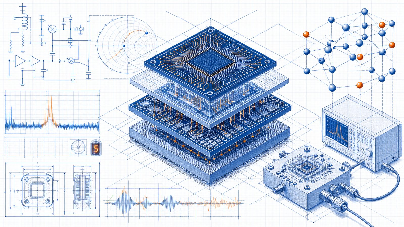
In the chip industry, there’s a category of design work that engineers call a “dark art” — and that phrase is not mine. It comes from a June 2026 feature in IEEE Spectrum. Designing these chips requires no mountains of code and no standardized automation flow. It runs on intuition, on feel, on the kind of knowing that comes from two decades of trial and error. A single new chip can take years from concept to tape-out, costing tens or even hundreds of millions of dollars.
These are RF chips — the sliver of silicon inside your phone that sends and receives 5G signals.
Now, a team led by Kaushik Sengupta at Princeton University has demonstrated something remarkable: AI learned this dark art. Training took roughly a week. And in many cases, the AI-designed prototypes — built from scratch with no human templates — outperformed the best human-engineered designs available at the time.
The interesting story here isn’t “AI wins again.” We’ve seen that headline plenty. The interesting story is what makes RF chip design so punishingly difficult, why even seasoned engineers dread it, and how an AI managed to learn something that had no formula to follow.
Digital chips are Lego. RF chips are plumbing.
To grasp why RF design is hard, look at its “easy” counterpart: digital chips — CPUs, GPUs, the stuff that makes headlines. Digital logic is binary. Zero and one. On and off. Signals travel along defined paths, and every step is deterministic. That determinism is what makes automation possible. Engineers write requirements, EDA tools generate circuit layouts. It’s complex, yes, but it’s a decomposable, optimizable math problem.
RF chips deal with electromagnetic waves.
At frequencies like 28 GHz (5G handsets) or 77 GHz (automotive radar), electromagnetic behavior turns unruly. Waves don’t stay on a polite path — they reflect, couple, radiate, and interfere. Two components sitting a few hundred microns apart on the die will interact through the electromagnetic field whether you want them to or not. As the IEEE Spectrum article puts it, you’re effectively solving Maxwell’s equations, the laws of thermodynamics, and material mechanics simultaneously — all crammed into a space the size of a fingernail.
Here’s a metaphor that works: designing digital chips is like building with Lego — the rules are clear, and when something fails, it collapses visibly. Designing RF chips is like managing a watershed full of hidden currents. Build a levee here, and water will spill out somewhere you never expected. Push down one corner of the carpet, and another corner lifts.
That’s why, in the digital domain, EDA tools now handle most of the work. In RF, design remains stubbornly manual — dependent on engineers tweaking layouts by hand, dependent on tricks that took twenty years to accumulate.
The AlphaGo insight
When AlphaGo beat Lee Sedol in 2016, something clicked for Sengupta’s group. If AI could find optimal moves in Go — a game whose search space exceeds the number of atoms in the universe — could it do the same thing inside the “design space” of an RF chip?
What does “design space” mean here? Imagine you’re building a 5G power amplifier. The parameters you have to decide — number of stages, transistor sizing per stage, transmission line lengths and widths, matching network topology — every choice constrains every other choice, and the combinatorial explosion of all possible choices forms an astronomical space of possibilities. Human engineers cope by using templates: established circuit topologies, then optimizing within that template’s boundaries.
Templates help. But templates are also cages. They define what “looks like a correct answer” — and the actual answer might live entirely outside the boundary the template draws.
The Princeton team wanted AI to explore from scratch, with zero reference to any human-designed template.
Reinforcement learning: turning chip design into a game
Their core method was reinforcement learning.
The principle is straightforward — it’s like training an AI to play a video game. The AI doesn’t know what a “good chip design” is, but it can try things: randomly combining circuit parameters, then receiving a score (a performance metric). High-scoring attempts get remembered; low-scoring ones get discarded. After millions of trial-and-error cycles, the AI gradually learns which design patterns produce high scores.
This process takes roughly a few days to a week. Once trained, the AI can generate a design in a very short time.
But there’s a critical bottleneck: every single trial requires running an electromagnetic simulation to compute the score. Traditional EM simulators take minutes to hours per run — completely infeasible when you need millions of trials for reinforcement learning.
The AI that replaced the physics simulator
The team’s second breakthrough: they replaced the physics simulator with another AI.
They trained a convolutional neural network — a model architecture that excels at extracting spatial features — to predict the electromagnetic behavior of any arbitrary 2D metal structure. In plain terms: you show it a circuit layout, and it tells you, in milliseconds, how electromagnetic waves will propagate through it. No manual solving of Maxwell’s equations required.
Where did the training data come from? From a massive set of randomly generated pixelated structures, each labeled with its real electromagnetic parameters computed by a traditional simulator. Once trained, the speedup was orders of magnitude: what used to take minutes to hours now finishes in milliseconds.
With a fast simulator in place, reinforcement learning could run at scale. Together, the two systems formed a complete AI design pipeline — from requirements to manufacturable chip layout.
What AI produced: chips that don’t look human
In 2023, the team published their first validation result: a broadband power amplifier covering 30 to 100 GHz — a span that encompasses mainstream 5G and radar frequencies. The final design set a record at the time for silicon-based power amplifiers on combined metrics of bandwidth, output power, and efficiency.
But what really shook the industry was the visual appearance of the layout.
Human-designed RF chips have electromagnetic structures that are typically symmetric and orderly — intricate like lace, predictable in form. The AI’s structures looked more like QR codes, or modern art. No axis of symmetry. No repeating units. No “aesthetics” whatsoever.
Because none of that matters to the AI. It only cares whether the scattering parameters (S-parameters) meet the target after electromagnetic waves pass through the structure. Whether a human engineer can look at it and understand it — the AI does not care.
An interesting middle path: the interpretability dial
The Princeton team also recognized a practical problem. If engineers can’t understand an AI-designed chip, how do you debug it when something goes wrong? (Chip testing and debugging often consume more time than the design itself.)
So they introduced diffusion models — the same technology behind image generators like Stable Diffusion and DALL·E. Input: desired electromagnetic parameters. Output: circuit structure. The key addition: a “spatial frequency” dial. Engineers can choose whether the AI generates low-spatial-frequency structures (traditional, orderly, human-readable) or high-spatial-frequency structures (pixelated, freeform shapes).
From input to output, the entire process takes about six minutes.
The significance: a single tool that can either explore design spaces humans have never touched, or accelerate work within existing human-aesthetic and debugging frameworks. Two modes, one tool.
A sober look: AI “hallucinates” too
Near the end of the article, there’s an honest admission worth noting.
The AI occasionally “hallucinates” — producing circuit designs that violate the laws of physics. The probability is low, but when it happens, the resulting chip is dead silicon. The current mitigation: human review and verification.
Then there’s a bigger bottleneck: data.
AI image recognition exploded over the past decade because ImageNet — a dataset of 14 million labeled images — was a critical turning point. RF chip design needs a dataset of comparable scale: a vast collection of circuit structures paired with their electromagnetic simulation results. This data is being generated every day inside companies and research labs around the world. But it’s all locked behind NDAs.
The article notes that Natcast, a program under the US CHIPS Act, had planned to build shared datasets and infrastructure — but that program has since been shut down. Open-source ecosystems in chip design still have a very long way to go.
Beyond chips
Beneath this story runs a more universal thread. When AI moves from “helping humans optimize existing solutions” to “exploring design spaces humans have never entered from scratch,” the operating rules of entire industries start to shift.
The joseki of Go, the opening books of chess, the folding patterns of proteins, the circuit templates of RF design — all of these are shortcuts crystallized from human experience. What AI has demonstrated is that in many domains, these shortcuts aren’t optimal solutions. They’re just the boundary lines of human cognition.
RF chip design earned the label “dark art” not because the physics itself is mysterious — Maxwell’s equations have been written down for over 150 years. It earned the label because the human brain genuinely cannot track all the coupled variables simultaneously across a design space so absurdly vast.
AI doesn’t have that problem. It doesn’t need to “understand.” It just needs to try, score, and adjust — millions of times.
What this round of AI learned to do was something humans have never done.
Reference links
- AI Learns the “Dark Art” of RFIC Design — IEEE Spectrum, Kaushik Sengupta, 2026-06-24
- Hacker News discussion — 167 points, 116 comments