On September 14, 2026, Fujitsu unveiled its next-generation server CPU, MONAKA, manufactured on a leading-edge 2nm process, alongside an accompanying line of enterprise server hardware. In marketing targeted at enterprise and defense sectors, this slice of silicon was pitched as a landmark achievement in reclaiming Japanese technological sovereignty—quickly surging to the top of Hacker News with 476 points.
“Monaka” refers to a traditional Japanese wafer cake filled with sweet red bean paste. Fujitsu deliberately chose this name to firmly tether the narrative of pure Japanese domestic manufacturing to this piece of silicon.
Beneath this sugarcoating of national ambition lies a sophisticated yet unyielding industrial reality: Japan can independently design, name, and assemble a flagship 2nm processor, but etching it onto silicon wafers still depends on overseas foundry capacity within TSMC’s orbit. Sidestepping American technological dominance does not mean escaping the global division of semiconductor labor; the sovereignty bottleneck has merely shifted from architectural blueprints down to advanced lithography cleanrooms.
Red Bean Pastry Naming Cannot Mask the ARMv9 Core
During the launch event, Fujitsu aggressively touted MONAKA’s single-node throughput, claiming up to twice the performance of competing general-purpose CPUs in AI inference workloads.
On paper, the specifications are formidable. Clock speeds reach up to 3.8 GHz, delivering single-precision floating-point throughput between 4.3 and 6 TFLOPS. To harness this computing power, the chip provides full support for the SVE2 vector instruction set and integrates dedicated hardware acceleration modules optimized for matrix operations.
Baking matrix math units directly into general-purpose processors has become the industry standard for handling small-batch LLM inference. Using traditional scalar instructions for tensor matrix multiplication is like firing a single-shot rifle, whereas dedicated matrix acceleration upgrades the firepower into broad-area coverage, dramatically driving up floating-point throughput per clock cycle.
Yet in international tech communities, top-voted comments cut through the corporate spin to expose a foundational truth Fujitsu downplayed: bite through the sweet red bean filling of this Japanese pastry, and the underlying instruction set running the code remains standard ARMv9 architecture.
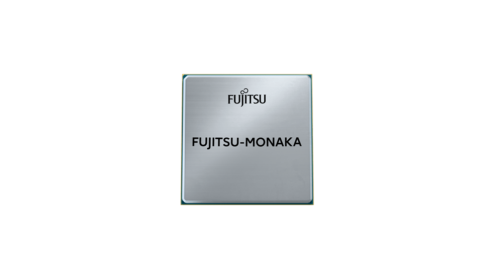 Figure: Official product render of the FUJITSU-MONAKA CPU. Source: Fujitsu press release
Adopting a standard ISA is not an engineering surrender; it is a pragmatic concession to the software ecosystem. To ensure frictionless deployment across enterprise and defense infrastructures, Fujitsu incorporated Arm CCA (Confidential Compute Architecture), leveraging hardware-enforced encryption to safeguard data in memory. This hardware-grade memory isolation physically shields workloads from malicious snooping—a non-negotiable ticket for entry into European and Japanese sovereign cloud data centers.
Squeezing 844 GB/s Per Socket: Bridging the VRAM Chasm with CXL
On the modern LLM inference battlefield, raw compute is rarely the primary barrier; memory bandwidth is the true bottleneck determining life or death.
MONAKA’s answer is a 3D chiplet packaging architecture combining diverse functional dies. Expensive, leading-edge 2nm capacity is reserved exclusively for compute cores starved for processing power, while cache and I/O modules are relegated to a more economical 5nm node. This heterogeneous stacking reserves precious EUV lithography machine time for where it matters most, slashing single-chip manufacturing costs without sacrificing aggregate throughput.
On the I/O side, the processor maxes out 12 memory channels supporting high-spec DDR5 RDIMMs running at 8800 MT/s, pushing aggregate socket bandwidth to a staggering 844 GB/s.
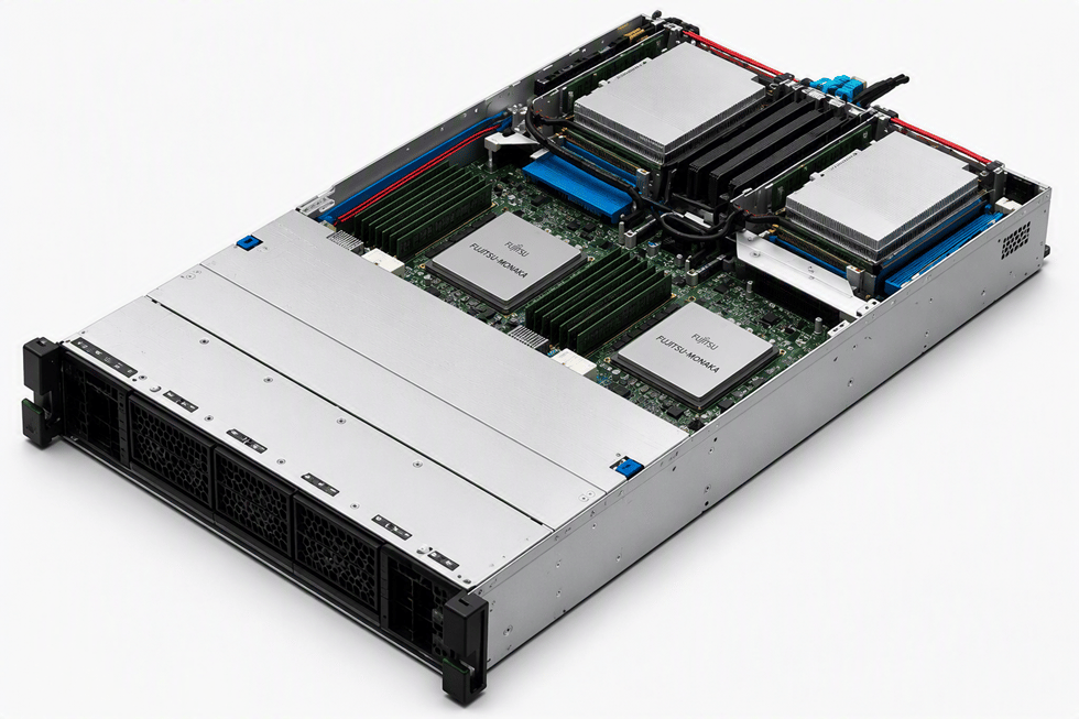 Figure: Official product render of the Fujitsu MONAKA Server. Source: Fujitsu press release
While this figure falls short of the extreme bandwidth offered by GPU-bound HBM stacks, it represents an unprecedented highway in the realm of general-purpose servers. An exceptionally wide physical bus directly alleviates the “memory wall” that Transformer architectures repeatedly hit during the token decoding phase, ensuring the CPU no longer stalls on memory transfers while generating long text streams word by word.
To digest this immense throughput, Fujitsu’s 1U and 2U servers integrate CDI (Coherent Device Interconnect) and CXL (Compute Express Link) high-speed interconnect architectures. In the 1U chassis, the system dynamically pools host memory alongside external accelerators.
Pooling memory fundamentally decouples a node’s physical memory ceiling from motherboard DIMM slots. When an inference cluster encounters sudden traffic spikes or out-of-memory errors, nodes can borrow memory dynamically across the CXL pool rather than crashing or forcing operators to purchase expensive dedicated accelerator clusters.
45°C Water Inlet Tolerances: Rewriting Data Center Cooling Economics
Pinning thermal envelopes and power consumption strictly within tight bounds is where this 2nm chip truly seeks to outmaneuver the competition from an engineering standpoint.
Massive AI compute clusters today routinely demand costly, complex liquid-cooling infrastructures. In contrast, MONAKA servers can operate reliably on standard air cooling in ambient temperatures up to 40°C. When switched to liquid cooling, the system can digest warm inlet water temperatures up to 45°C.
Raising inlet water limits by 5 to 10 degrees is a transformative economic lever for data center operators. Facilities no longer require energy-intensive chiller plants to maintain strict cold-aisle environments. Chiller compressor runtimes plummet, dropping facility PUE (Power Usage Effectiveness) by an entire tier.
Official benchmark estimates indicate that this thermal design can cut server cooling power consumption by up to 80%. This precipitous drop in cooling overhead serves as Fujitsu’s primary selling point when pitching legacy clients across Europe and Japan.
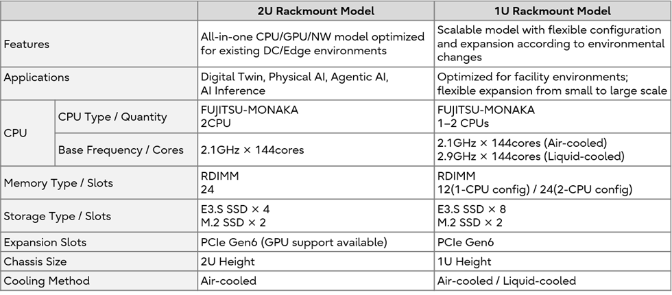 Figure: Schematic of the MONAKA server product line. Source: Fujitsu press release
Yet within high-density server racks, MONAKA exposes physical compromises. Developers in community discussions quickly highlighted a glaring architectural constraint: each MONAKA node supports a maximum of only two CPU sockets.
In an era where modern AI compute nodes routinely pack four to eight accelerators per chassis, a dual-socket ceiling arrives prematurely. When customers need to cram maximum compute density into standard racks, this socket limitation forces them to buy more physical chassis—spending the electricity savings right back on additional rack colocation and floor space leases.
Eighteen Years After Selling Its Fabs: The Sovereignty Reality Check
Behind this bespoke hardware and software stack stands funding and project backing from Japan’s New Energy and Industrial Technology Development Organization (NEDO). Final system assembly takes place at the Kasashima plant on Japanese soil, allowing Fujitsu to market a narrative of “end-to-end supply chain transparency and absolute traceability.”
Yet between “assembly-level transparency” and genuine “manufacturing sovereignty” lies a technological chasm that national sentiment alone cannot bridge.
Engineers versed in semiconductor history quickly pulled back the curtain in online forums: around 2008, Fujitsu sold off its core wafer fabrication facilities to UMC, severing its own capital-intensive manufacturing arm.
Eighteen years after shedding manufacturing capabilities, Japan lacks domestic commercial fab lines capable of mass-producing 2nm silicon. Even TSMC’s joint-venture JASM fab in Kumamoto was structured around mature process nodes first, with mass production of 2nm remaining a distant milestone.
While Fujitsu’s press release did not disclose the foundry partner, industry consensus points squarely to TSMC. No matter how elegant the architectural schematics appear on paper, printing billions of transistors using extreme ultraviolet lithography still hinges entirely on the global foundry supply chain controlled by a handful of giants—not on Japanese machine tools.
In 2008, Fujitsu’s 10Gbps network switches delivered peerless performance, prompting Google to purchase them en masse while building out its early packet-capturing infrastructure. But that marked the swan song for Japanese enterprise hardware in Silicon Valley; Fujitsu never again established a lasting foothold in American core infrastructure.
Today, MONAKA finds itself trapped once again in the historic fissure between national narrative and industrial reality. It boasts ingenious heterogeneous packaging, rigorous hardware-enforced memory isolation, and exceptional energy efficiency. Yet its physical silicon heart must inevitably be brought to life by overseas foundry giants.
As global computing infrastructure fiercely battles for advanced lithography capacity, national subsidies and domestic factory assembly cannot buy authentic technological sovereignty. What defines a nation’s computing baseline is not the poetic pastry named on an architectural blueprint, but the relentless hum of advanced wafer fabs running day and night.
References:
- Fujitsu Press Release
- Hacker News Discussion