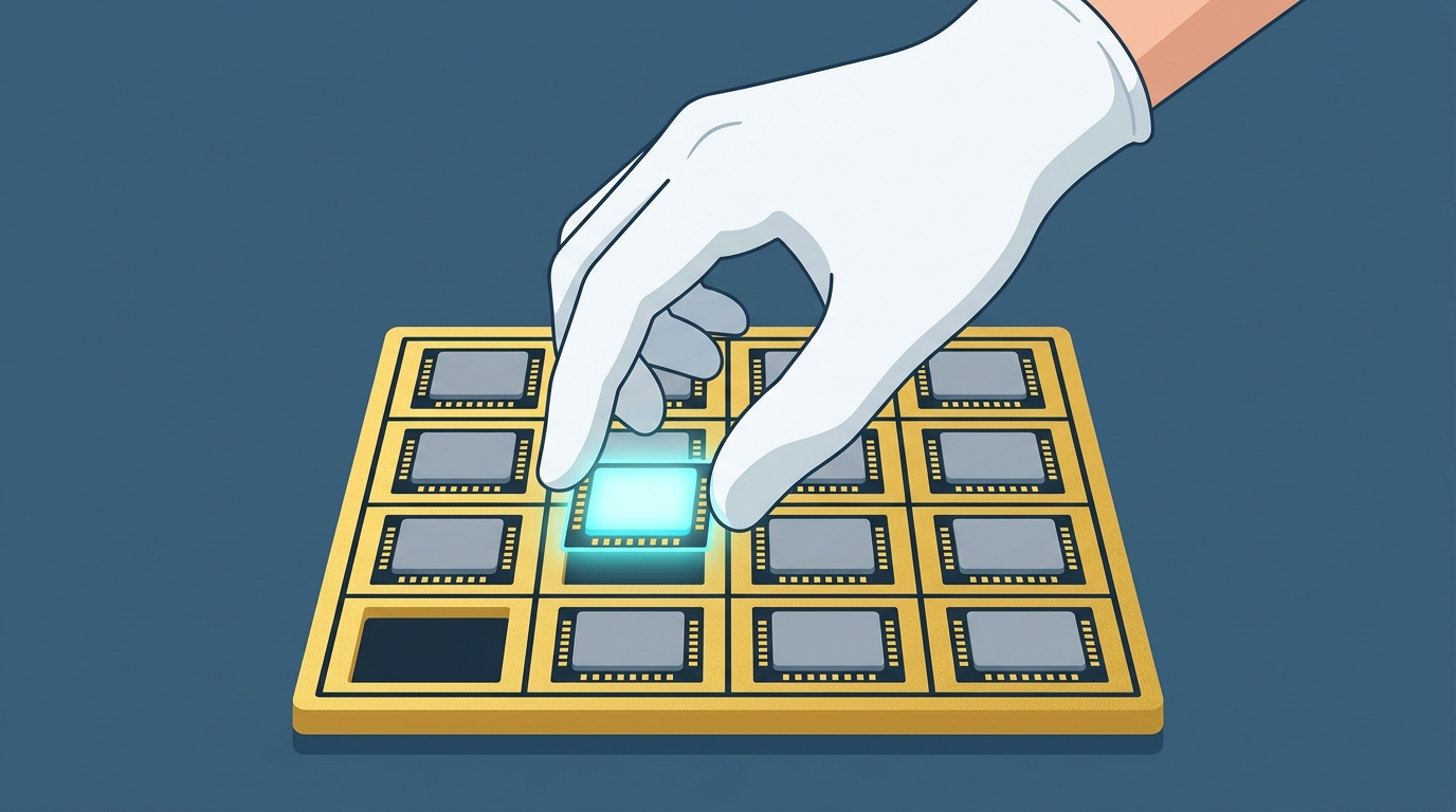
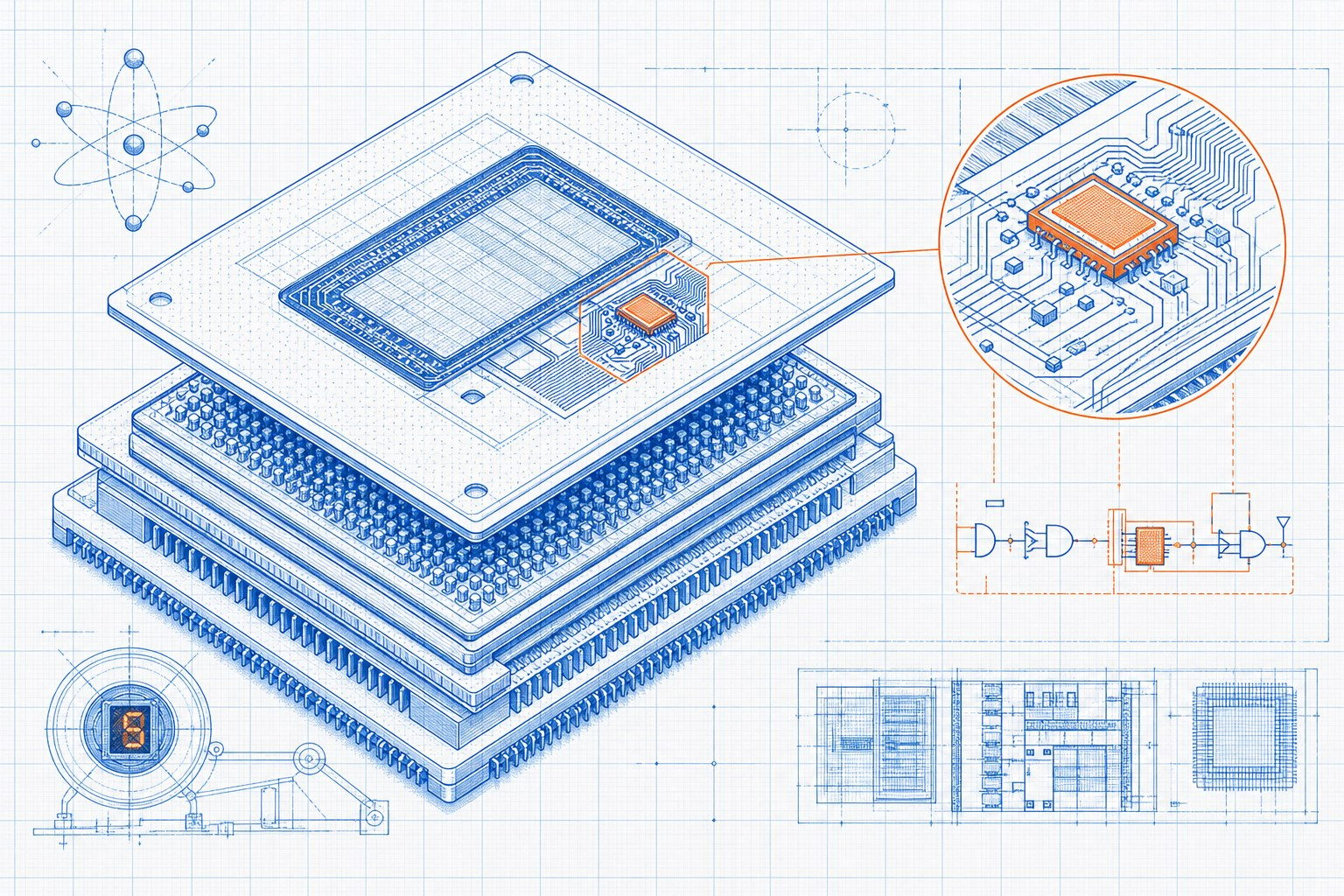
On June 25, 2026, at IBM’s Yorktown Heights facility in New York, the company dropped a headline that lit up tech media across the board: the world’s first sub-1nm chip technology. 0.7 nanometers — or 7 ångströms — a scale approaching the diameter of a single silicon atom. In the press release, IBM Research director Jay Gambetta called it “a milestone moment in computing.”
Meanwhile, in the Hacker News comment section, a group of users with electrical engineering backgrounds were busy pixel-peeping the die micrographs IBM had released.
One highly-upvoted comment captured the essence of this quiet standoff with precision: “They actually delivered a ‘nanostack’ architecture built with roughly 5nm features, then told you this is effectively equivalent to a theoretical sub-1nm chip. The tech itself is interesting, but this industry has a few too many marketing people.”
This isn’t a simple “breakthrough: real or fake?” debate. The naming of semiconductor process nodes is, in itself, one of the longest-running battles over language and legitimacy in the tech industry’s last thirty years.
Node Naming: From Physical Dimensions to Virtual Code Names
To understand the subtext of this controversy, you need to go back to where semiconductor node naming began.
In the industry’s early days, node names did correspond to a real physical dimension on the transistor — typically the gate length (Lg). Intel marched from 10 microns in 1972 to 0.35 microns in 1995. Across those 23 years, the node name and the gate length matched precisely. “250 nanometers” at the time genuinely meant the chip’s most critical physical structure was 250 nanometers.
But the inflection point arrived in 1997. At its 250nm node, Intel fabricated gates at 200nm — 20% better than the name implied. Over the next 12 years, this “over-delivery” kept widening: at the 130nm node, gate length was only 70nm — roughly half the name.
In 2011, the script flipped. When Intel introduced its 22nm node, gate length was 26nm — nearly 20% larger than the name. From that point, node naming entered what could be called the “exaggeration era”: at the 10nm node, gate length was about 18nm, nearly double the name.
EEJournal’s Kevin Morris, in his 2020 article No More Nanometers, delivered a sober summary: “Since 1997, the node name hasn’t represented any actual dimension on the chip, and it has deviated by nearly a factor of two in both directions.” In 2020, TSMC vice president Y.J. Mii published a paper in IEEE Proceedings formally proposing that density metrics replace the outdated “nanometer” nomenclature — even a competitor of Intel, the company most burdened by the naming game, believed the system had outlived its usefulness.
That’s the historical context into which IBM’s announcement is embedded. When an industry has used the word “nanometer” for thirty years to describe progress, and the word has long since detached from physical reality, every new node announcement is destined to become a battle over definitions.
What IBM Actually Announced
Setting aside the “0.7 nanometer” headline number, the technical substance of IBM’s announcement runs roughly as follows.
The core is a novel transistor architecture called “nanostack.” Building on GAAFET (Gate-All-Around) nanosheet transistors, IBM uses 3D sequential integration to stack transistors vertically in an interleaved arrangement. As IBM describes it, nanostack has been experimentally validated across three dimensions: ultra-thin dielectric bonding for CMOS integration, dual-channel engineering, and switching performance of functional CMOS inverters — results that collectively demonstrate the architecture can be physically fabricated and perform real computation.
At the VLSI 2026 conference, IBM also presented SRAM data: the nanostack architecture achieved over 40% SRAM cell area reduction. A chip the size of a fingernail integrates nearly 100 billion transistors, roughly double the density of IBM’s 2nm chip announced in 2021. On performance, IBM claims a 50% performance improvement or 70% energy efficiency gain over the 2nm node.
An easily overlooked detail: IBM’s own press release contains the line — “while transistor nodes now refer to manufacturing technology generations rather than exact physical dimensions.” Publicly, IBM doesn’t pretend “0.7 nanometers” is a literally measured length. But the headline and promotional framing still make “sub-1nm” the centerpiece, and this very tension is what ignited the community discussion.
IBM’s standing in semiconductor R&D is also genuinely significant. It was among the first institutions to invent nanosheet technology, and its Albany research facility is about to install ASML’s High NA EUV equipment. IBM is simultaneously collaborating with Lam Research, Tokyo Electron, SCREEN, and other equipment vendors on supporting processes. These partnerships demonstrate that IBM isn’t talking into the void — it is genuinely pushing the boundaries of physical manufacturing capability.
But the problem is that the distance between “lab demonstration” and “commercial volume production” is often orders of magnitude larger than the numerical jump from “2 nanometers” to “0.7 nanometers.”
The Technical Community’s Skepticism: Three Key Anchors
The skepticism in the HN comments largely clusters around three directions.
The first direction is physical limits. User adrian_b noted that for silicon, there exists a physical lower bound for FET gate length, roughly between 10nm and 15nm. The most advanced CMOS processes today haven’t even reached this limit. To truly shrink a transistor below 1 nanometer would require semiconductor materials beyond silicon. The “dual-channel engineering” mentioned in IBM’s nanostack may hint at new materials, but the public disclosures don’t specify the actual channel material combination. Another user directly analyzed IBM’s released micrographs: the scale bars appeared inconsistent — the rightmost image’s scale bar was less than half that of the middle image (~10nm), but the magnification was clearly more than double, and the circled “silicon atom rows” were calculated to be at least 1.6nm wide.
The second direction concerns dimensional cheating. Multiple commenters pointed out that vertical dimension control has long been achievable at atomic precision (dependent on thin-film deposition rate and time, not lithographic resolution), but circuit density is primarily determined by horizontal feature sizes. As adrian_b wrote: “Vertical dimensions of ~1nm or even smaller have been achievable for decades because they depend on growth rate and time, not lithography like horizontal dimensions do.” Equating the area-equivalent density gains from 3D stacking with traditional 2D scaling is a genuine reflection of technological progress, but conflating the two in naming is misleading — after all, the performance benefits of 3D stacking and the physical implications of 2D scaling don’t fully correspond.
The third direction leans on industry experience. IBM sold its wafer fabrication business to GlobalFoundries back in 2014 — not only sold it, but paid $1.5 billion for GlobalFoundries to take it. Since then, IBM has maintained significant semiconductor R&D capabilities, but its role is defined by “research without production”: develop technology, file patents, license them out. This means the gap between IBM’s published technology roadmap and actual foundry mass-production timelines is still mediated by the enormous chasm of technology transfer and process integration. One comment distilled this sentiment succinctly: “Nobody knows for sure what IBM’s definition of ‘sub-1nm’ actually means. And IBM does more hype than any company in the industry, so nobody bothers to study what they actually said.”
What Actually Deserves Attention
If we accept the premise that “nanometer numbers” have long been a marketing symbol, then the genuinely informative parts of IBM’s announcement aren’t in that number.
First is 3D sequential integration. The “stack upwards” approach that nanostack represents — building transistors layer by layer in the vertical direction — differs from the industry’s current mainstream 3D integration path via advanced packaging (e.g., chiplets). If IBM’s bonding technology and channel engineering can be validated as production-viable, it genuinely opens a new dimension of density growth.
Second is SRAM shrinkage. At advanced nodes, SRAM cell area scaling has significantly lagged logic area scaling, becoming one of the bottlenecks for cache bandwidth in AI chip design. If the nanostack architecture can deliver a 40% area reduction in SRAM, the impact on high-bandwidth AI compute workloads may be more practically significant than the logic density number.
Third is the timeline. IBM’s roadmap points toward the 2030s — nanosheet GAAFET’s projected lifespan is about five to seven more years. This means nanostack is a candidate for the post-GAA era, at least five to seven years away from production. Some analysts note that imec (the independent nanoelectronics research center in Belgium) predicts GAAFET will reach its limits in the early-to-mid 2030s; IBM’s announcement is laying the groundwork for a successor technology when that time comes.
These engineering developments deserve industry attention, but their connection to the “0.7 nanometer” number is more a matter of naming convention inertia than a breakthrough in physics.
The Naming Dilemma and Industry Inertia
Perhaps the most intriguing point is that virtually everyone in the industry agrees the node naming system is broken, but no one can actually end it.
A recurring suggestion is to replace the nanometer number with transistor density (millions of transistors per square millimeter, MTr/mm²). This metric is intuitive, unfakeable, and comparable across foundries. But the problem is that density is a precisely calculable number — and precise numbers are bad for marketing. As one user wrote: “If they switched to concrete numbers, they could no longer claim their ‘1nm’ process is better than someone else’s ‘2nm’ process — if the density isn’t actually better.”
This dilemma won’t change because of a single IBM announcement. It ultimately depends on whether consensus can form among the major foundries (TSMC, Samsung, Intel) and industry roadmap organizations. Until then, every new node announcement will keep repeating this language game.
And the best thing consumers and investors can do is, the next time they see a headline with “point-something nanometers,” ask one more question: what exactly is this nanometer referring to?
Author’s note: This article is based on IBM’s official announcement of June 25, 2026, and the Hacker News community discussion. All HN user comments quoted are publicly posted content. I hold no stock or financial interest in IBM, TSMC, or any related company. Semiconductor technology evolves rapidly; this analysis reflects only publicly available information as of publication time.