You’re a physical implementation engineer at a chip design company. It’s 2 AM. The EDA tool just finished the latest round of place-and-route. The utilization number on your screen reads 92% — but you know in your gut that the remaining 8% of die area can’t possibly squeeze in the next group of standard cells. The n-type and p-type transistors are already cheek-to-cheek; one step closer, and crosstalk and leakage will eat your timing margins alive.
The limit of planar layout has arrived.
This isn’t a single process node’s problem. For fifty years, Moore’s Law’s driving logic was roughly the same: make transistors smaller, shrink the pitch, cram more devices into the same area. But from FinFET to GAA (Gate-All-Around), the essence of every architectural upgrade has been finding balance between “gate control over the channel” and “continued physical shrinkage.” And when gate pitch shrinks to the tens-of-nanometers scale, the traditional CMOS layout — n-type and p-type transistors sitting shoulder-to-shoulder on the same plane — becomes itself the new bottleneck.
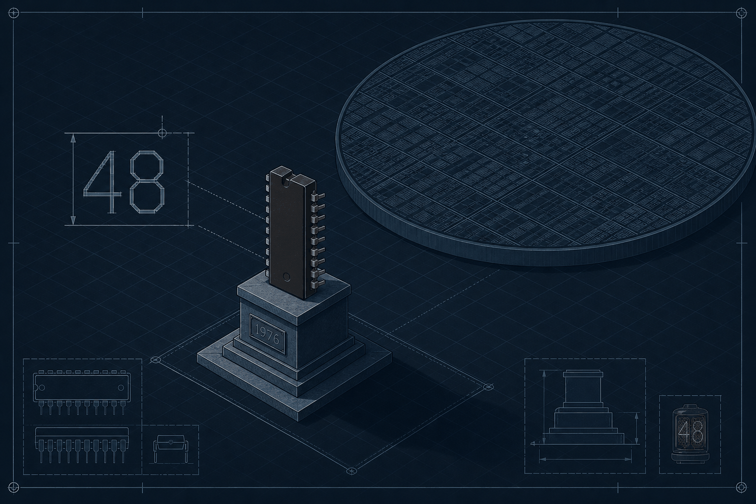
From June 14 to 18, 2026, the VLSI Symposium was held in the United States. Samsung Electronics’ Semiconductor R&D Center presented a paper with a title as long as academic convention demands: “First Demonstration of 3D Stacked FETs at Gate Pitch of 42 nm Featuring Triple Stacked Nanosheet Channels for Advanced Logic Applications.” But beneath the verbose title lies a simple answer: if you can’t fit any more on the plane, build upward.
From Single-Story to High-Rise: Four Generations of Transistor Architecture
To understand the significance of Samsung’s demonstration, we need to review what transistor architecture has been through.
Planar FET was the original form. The gate lies flat on a plane, controlling channel conduction and cutoff from one side. The advantage: simple process. The disadvantage: as the channel got shorter, gate control dropped off a cliff — leakage went from “tolerable” to “unacceptable.”
FinFET was the first borrow from the third dimension. The channel “stood up” from the plane into a thin fin, with the gate wrapping around three sides, dramatically improving control. Intel first commercialized FinFET at the 22nm node in 2011; the rest of the industry followed. FinFET sustained over a decade, all the way to 5nm and 4nm nodes.
GAA (Gate-All-Around) is step two. In FinFET, the gate wraps three sides of the fin, but the bottom side still touches the substrate — control isn’t truly “all around.” GAA makes the channel into bundles of horizontal nanosheets, with the gate completely wrapping each nanosheet from all four sides. Samsung was first to commercialize GAA at the 3nm node in 2022; TSMC introduced GAA at N2 in 2025.
3D Stacked FET is step three — and what Samsung showed at VLSI 2026. It no longer just stacks channels; it vertically stacks the n-type and p-type transistors. In a traditional layout, a CMOS logic gate requires one n-FET and one p-FET placed side by side; in 3D stacked FET, they become upstairs and downstairs neighbors. Same logic function, halved chip area.
Samsung’s official blog used an apt urban planning analogy: when a city runs out of land, planners don’t keep shrinking the gaps between buildings — they start building high-rises. Transistors on a chip face exactly the same dilemma.
42nm Gate Pitch: The Engineering Behind the Number
At first glance, 42nm might not seem impressive — TSMC and Samsung’s GAA production nodes already use smaller gate pitches. But 42nm means something entirely different here.
First, this is the smallest gate pitch achieved on a 3D stacked FET architecture. Previously, Intel demonstrated CFET (Complementary FET, the industry’s generic term for 3D stacked FET) at IEDM 2023 with a 45nm gate pitch. Samsung pushed it to 42nm, more compact than Intel’s result. In semiconductors, 3nm is enough to put a company a full step ahead.
Second, Samsung used triple-stacked nanosheet channels — each of the two vertically stacked transistors has three layers of nanosheets, totaling six layers of channels stacked vertically. This is the largest number of nanosheets ever demonstrated in the 3D stacked FET space. More channel layers mean more drive current per unit area, but maintaining crystal quality and dimensional uniformity across layers also gets harder.
Third, the paper scored 8.29/10 in peer review out of over 1,000 submissions, winning VLSI 2026 Best Paper and being selected for the symposium’s official technology highlights and media press kit. Reviewer recognition and process demonstrability are two different things; Samsung accomplished both in this paper.
Three Engineering Problems, Three Solutions
Samsung’s blog breaks the engineering challenges of 3D stacked FET into three categories — a framing that itself is worth noting, because it explains “why this isn’t simple.”
First: the current path can’t shrink. Stacking two transistors saves area, but if the channels are too narrow and drive current insufficient, transistor switching speed suffers. Samsung’s solution is triple-stacked nanosheets — three channels in parallel, equivalent channel width maintained, total footprint dramatically reduced. Stacking here plays two roles simultaneously: saving area and maintaining performance.
Second: crystal quality must be uniform across layers. In a multi-layer nanosheet structure, any layer with lattice defects or thickness variation causes uneven current distribution across layers — some layers overload, others idle, overall performance degrades. Samsung’s paper demonstrates precise optimization of the epitaxial growth process, achieving highly uniform, nearly defect-free silicon crystal channels across layers.
Third: upstairs and downstairs need soundproofing. With n-FET and p-FET vertically stacked, the extremely close physical proximity creates parasitic coupling risk. Samsung introduced a Middle Dielectric Isolation (MDI) layer that electrically separates the upper and lower transistors completely. MDI thickness and position must be extremely precise — too thin and isolation fails, too thick and the upper transistor’s gate structure formation is compromised. Samsung’s blog acknowledges that MDI’s importance is “equally critical” to the stacking technology itself.
Heat: What HN’s Comment Section Cares About Most
Samsung’s paper and blog are all about “how to make it,” but Hacker News’s comment section zeroed in on a different anxiety: heat.
User RicoElectrico’s top-voted comment: “What about heat dissipation? The number one problem with chips right now is heat, and higher density only makes it worse.” This anxiety isn’t armchair worrying. 3D stacked FET, by stacking two transistors vertically, doubles the heat flux per unit area while making the thermal conduction path more complex — heat from the lower transistor must travel through the middle isolation layer and the upper transistor to reach the heat dissipation structure.
The technical discussion in the comments went deep. mota7 noted that 30%–50% of modern chip thermal budget comes from leakage current, and leakage worsens with rising temperature — a positive feedback loop. mrandish was more pessimistic: “A significant fraction of the density gains from CFET may be unusable in practice due to thermal bottlenecks, unless new high-thermal-conductivity materials are found.”
But there were dissenting views. juancn argued that 3D stacking shortens interconnect lengths between transistors, and signal propagation time reduction is itself a power optimization: “On-chip signal propagation delay is becoming a problem. Huawei’s Logic Folding, TSV stacking, and others are all attacking from the shorter-path direction.” deepSun was more direct: “If most heat comes from conductor resistance, shorter paths equal less heat.”
These discussions point to a more fundamental question: how much of 3D stacked FET’s density gains can actually translate into chip performance improvements, and how much gets eaten by thermal bottlenecks? Samsung’s 42nm paper doesn’t answer this — it’s a “first demonstration” paper proving feasibility, not engineering limits. But the answer to this question will determine 3D stacked FET’s production timeline.
Samsung vs. TSMC: The Next-Gen Transistor Race
3D stacked FET isn’t Samsung’s solo road. The industry’s generic term is CFET (Complementary FET), and TSMC disclosed lab-stage CFET research results as early as its 2023 European Technology Symposium. TSMC then showed a CFET prototype at 48nm gate pitch and stated the technology “still requires many generations before entering mass production.”
Samsung has now pushed gate pitch to 42nm, numerically ahead of TSMC’s public results by a step. But the transistor race has never been decided by lab data alone — production yield, process stability, EDA toolchain support, customer design ecosystem — each of these is a longer battle.
Samsung already got a head start on GAA commercialization. In 2022, Samsung introduced GAA architecture first at the 3nm node, roughly three years ahead of TSMC (which only switches to GAA at N2, expected in H2 2025). But the first-mover advantage didn’t translate into market share — TSMC remains far ahead in advanced-node customer ecosystem and yield control. Will the CFET race repeat the same script? Too early to say.
From a technology roadmap perspective, Samsung’s positioning is clear: 3D stacked FET is a natural extension of GAA, not a departure. Samsung’s blog states: “GAA architecture naturally supports the transition to three-dimensional integration. GAA devices use nanosheet channels that can be formed in multiple layers, providing the technical foundation for vertical stacking and channel control.” It positions 3D stacked FET as the next step in GAA platform evolution into the third dimension, without drawing a “GAA era is over” dividing line.
This passage is simultaneously a roadmap declaration: Samsung is telling the industry it has already prepared GAA process experience for the CFET era.
Moore’s Law Is Still Breathing
There’s a category of technological progress whose significance lies in proving that something previously thought “maybe possible” is, in fact, possible.
The first demonstration of 3D stacked FET at 42nm gate pitch falls into this category. It doesn’t mean the chip in your phone next year will suddenly be twice as fast — production timeline, yield, thermal, EDA toolchain — each of these needs years to resolve. But it does mean one thing: when planar CMOS scaling finally hit the physical wall, the path of building upward is viable. Triple nanosheets, MDI isolation, 42nm gate pitch — these three terms together form one of the best semiconductor engineering statements of 2026.
From FinFET to GAA to 3D stacked FET, transistors keep getting taller. Moore’s Law has found a new way to live — no longer just “make things smaller,” but “build taller buildings on smaller plots of land.”
This article draws on publicly available information and community discussions. If you have deeper first-hand experience with this topic, corrections and additions are welcome.