In November 2026, chip research team Architect Labs unveiled a new milestone: an autonomous swarm of AI agents designed a complete, functional CPU from scratch. Throughout the entire R&D process, human engineers provided zero microarchitectural instructions—the algorithms independently deduced every architectural detail of the processor.
Fabricated on a 7nm physical layout, the chip, codenamed Frostbite, delivered 4.59x the performance per watt of a conventional dual-issue in-order core across 25 benchmark workloads. While that efficiency gain sounds like science fiction, the engineering reality calls for sober evaluation. The baseline TCPU core measured just 0.895 mm², and the benchmark suite was limited to 25 workloads. This remains an early exploration of computational methodology rather than a mass-production commercial victory.
The true breakthrough lies in restructuring the chip design pipeline. For the first time, algorithmic deduction overturned the computing substrate that human cognitive habits had locked in for decades.
AI Takes Over Microarchitecture: Zero Lines of Human Instructions
Architect Labs previously introduced Project Redwood, where human experts defined the hardware architecture while AI handled circuit implementation, formal verification, and deployment. With Frostbite, the team stripped away human architectural presets entirely, letting AI agents explore native computational topologies on their own.
Early on, the agent swarm produced a 141-page architectural proposal outlining a programming model, runtime system, and high-level modular designs. But lacking physical process constraints, the initial estimations violated physical laws. Once the first-generation circuit code hit the floor, it had to be scrapped completely.
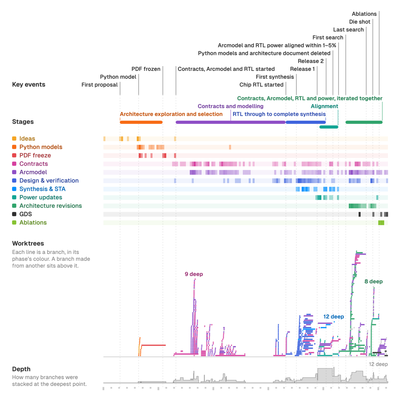 Figure: Complete development timeline from initial architecture proposal to final ablation. Source: architectlabs.com
Rather than reverting to manual human tuning, the engineering team built Arcmodel—a high-level formal system model that simulated hardware roughly 200x faster than low-level circuit simulation, with prediction errors strictly bounded within 5%. The entire model was formalized into over 800,000 lines of Lean mathematical contracts, eliminating logical loopholes at the formal source.
Interaction Nets Awaken After 36 Years: Half of Traditional Power Wasted on Tracking Dependencies
Frostbite’s energy efficiency stems primarily from replacing the foundational mathematical model of computation. Mainstream general-purpose CPUs rely on the von Neumann architecture, executing linear instruction streams. To squeeze out parallel performance, hardware burns millions of transistors at runtime guessing data dependencies, while multi-core systems maintain the illusion of shared memory through costly cache synchronization.
In the baseline dual-issue TCPU core, excluding clock tree dissipation, multi-level cache access consumed 57% of total energy. Instruction fetch, decode, and issue consumed another 27%. Combined, they accounted for 84% of total power, leaving minimal energy for actual arithmetic execution.
French computer scientist Yves Lafont introduced the theory of interaction nets at POPL 1990. In an interaction net, a program is not a linear sequence of instructions; it is a graph of interconnected nodes. Computation proceeds through local graph rewriting of adjacent active node pairs.
Each node possesses exactly one principal port. Active node pairs never overlap in graph space, meaning evaluation order cannot alter the final result—granting inherent, conflict-free concurrency. Furthermore, each value is consumed exactly once (linear logic), eliminating the need for hardware-level shared memory states.
This mathematical framework sat in academic archives for 36 years. Human programmers, accustomed to top-down imperative code, rarely write large-scale systems with graph rewriting semantics. AI agents carry no such cognitive biases: the algorithms compiled graph-oriented intermediate representations directly to hardware, bypassing traditional instruction pipelines.
Autonomous Work-Stealing: Halving Memory-Related Power
Free from out-of-order scheduling complexity, Frostbite assumed a radically different physical form. Instead of relying on a centralized controller to dispatch tasks, each compute tile operates autonomously based on three minimalist local rules.
Each compute tile first consumes active nodes from its local queue. When its queue empties, it actively requests work from neighboring tiles. If all adjacent neighbors have no work to spare, the tile immediately clock-gates itself into low-power sleep. This decentralized, work-stealing scheduler was never specified in human prompts; the agents synthesized it autonomously across iterative architectural evolutions.
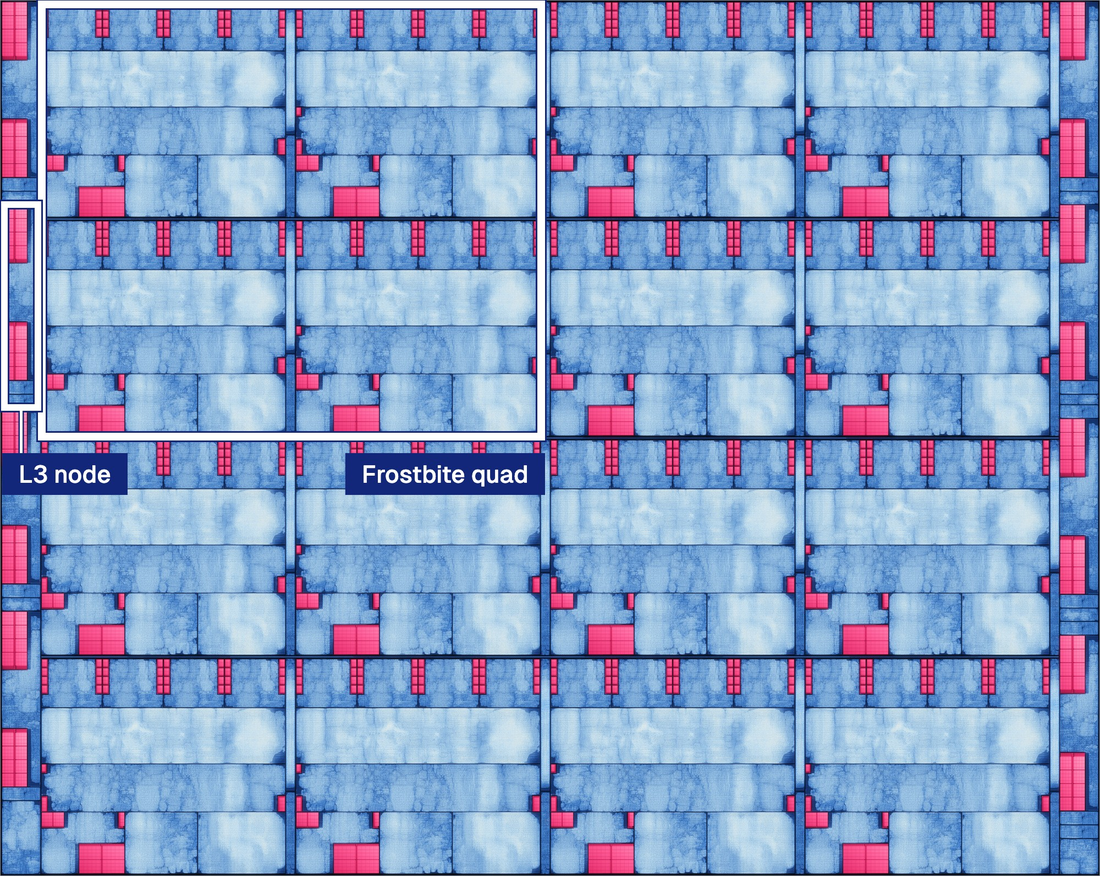 Figure: Physical layout at 7nm, highlighting a quad-core tile and L3 cache node in red. Source: architectlabs.com
Through explicit dataflow and localized memory, Frostbite reduced memory-access power consumption to 38% of the total budget. Fetch and decode overhead plunged from 27% to just 6%. To maintain the distributed mesh, the chip allocated 26% of its energy budget to the network-on-chip and node scheduling—a structural tradeoff that drastically increased effective computational efficiency.
In physical implementation, a Frostbite module comprising a quad-core tile and an L3 cache node measured 0.792 mm²—11.5% smaller than the baseline core. When scaled out to a 16-core array, energy consumption ratios remained stable, eliminating the cache coherency storms that plague conventional multicore scaling.
58 Iterations and 250% Error: How Formal Verification Kept Hallucination in Check
Autonomous evolution is not effortless magic. Over the design lifecycle, the agent cluster proposed 58 microarchitectural modifications. Rigorous ablation experiments accepted only 37 into the final physical layout.
The surviving modifications included runtime clock gating, more compact L3 cache directory entries, and shared functional extensions. None were arbitrary; every architectural change was validated with end-to-end performance-per-watt profiling.
In early iterations, AI-generated performance and power estimates diverged from physical reality by up to 250%. If left unconstrained, models guided solely by LLM intuition would have failed physical timing closure.
The engineering team’s automated calibration pipeline acted as a safety harness. The system continuously ingested precise ground truth from RTL physical simulations to calibrate the higher-level Arcmodel abstraction. Within two calibration rounds, system-level power and area discrepancies converged to under 5%, grounding every high-level exploration in physical silicon reality.
Behind 4.59x Energy Efficiency: A Methodological Milestone, Not a Mass-Production Triumph
Silicon measurements define the true boundaries of this architecture. Across 25 benchmark workloads, Frostbite achieved a geometric mean 4.59x improvement in performance per watt, alongside an 8.77x improvement in performance density per unit area.
Deconstructing the benchmark results reveals clear technological boundaries. On the 10 workloads used to guide architecture search, efficiency jumped 6.02x. On the 15 held-out workloads never seen during optimization, average gains settled at 3.83x. This confirms generalized gains for dataflow computing, alongside clear preferences for specific workload graph structures.
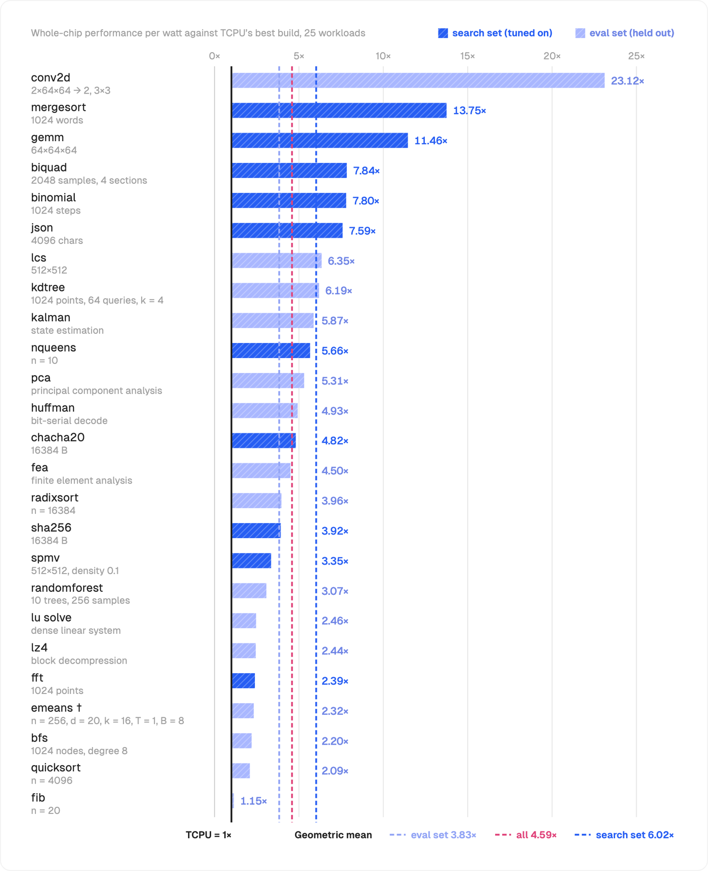 Figure: Energy efficiency distribution of Frostbite versus the conventional dual-issue core across 25 benchmark workloads. Source: architectlabs.com
Workload extremes are revealing: on regular 2D convolutions (conv2d), massive concurrency unlocked a 23.12x efficiency surge over the baseline. Conversely, on a Fibonacci benchmark laden with recursive branching and pointer indirection, efficiency gains dropped to 1.15x. Irregular call stacks slow down graph rewriting, highlighting the inherent challenge interaction nets face with arbitrary imperative code.
The choice of baseline is another crucial engineering caveat. The reference TCPU is an ultra-low-power dual-issue in-order core lacking heavy mechanisms like branch predictors and out-of-order execution engines. Against modern out-of-order multi-issue processors, the efficiency multiplier would look very different.
Architect Labs acknowledged that confidentiality agreements prevent disclosing the commercial identity of the baseline processor. The new instruction set architecture and hardware RTL remain proprietary, with FPGA prototyping and standard benchmark porting still underway.
Frostbite’s primary contribution is not defeating a specific silicon chip. Its significance lies in proving that algorithms can design processors unencumbered by human cognitive precedent. Decades-old mathematical theories can be materialized into physical silicon. When instruction sets no longer cater to human reading habits, hardware efficiency charts a completely new course.
Reference Links:
- Architect Labs Official Technical Report
- ACM SIGPLAN POPL 1990 Proceedings
- Computer Architecture and Formal Hardware Verification Literature