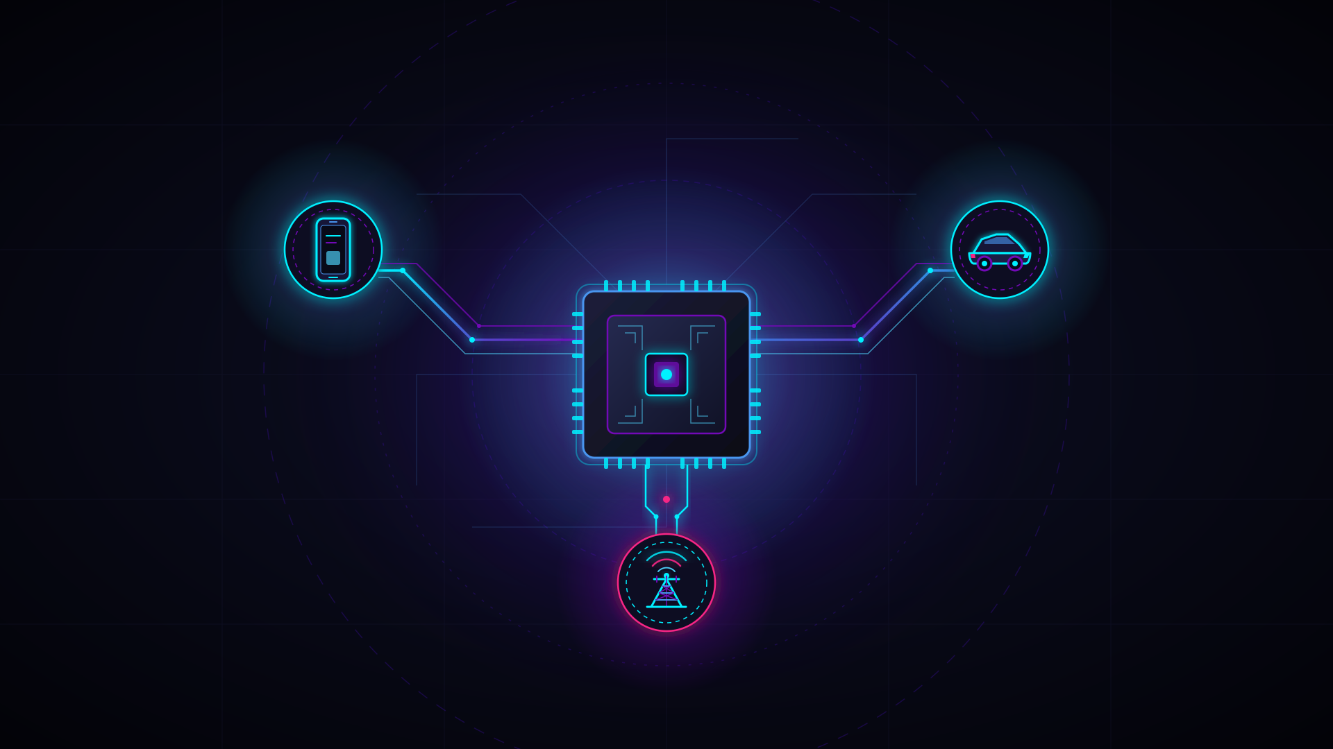
On October 4, 2026, Huawei Executive Director Richard Yu confirmed in a video address that Huawei has successfully engineered and mass-produced 381 semiconductor Tau ($\tau$) chips spanning mobile handsets, artificial intelligence, networking infrastructure, and intelligent automotive platforms. In an era where silicon-based semiconductor fabrication scaling faces escalating physical barriers, the company is deploying a distinct engineering paradigm to sustain the momentum of Moore’s Law.
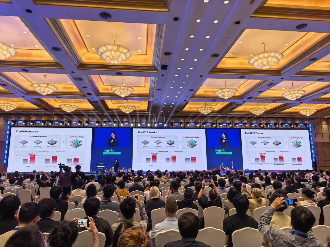 Figure: Architecture schematic of Huawei Tau chips. Source: Huawei official presentation.
Transistors Near Physical Limits: Turning to the Time Domain for Performance
The semiconductor industry’s conventional trajectory has long relied on continuously shrinking the physical dimensions of transistors—a paradigm known as “geometric scaling.” Along this path, engineers repeatedly iterated photolithography equipment to etch increasingly dense circuitry onto identical silicon die areas. However, as fabrication nodes advance down to mere nanometers and into the Angstrom regime, the physical landscape fundamentally shifts. Quantum tunneling effects and leakage-induced thermal accumulation create formidable physical roadblocks. Concurrently, the capital expenditure and operational costs for extreme ultraviolet (EUV) lithography systems have skyrocketed, while the marginal performance gains yielded per silicon wafer are sharply diminishing.
Confronted with this narrowing corridor, Teresa He (He Tingbo), President of Huawei’s semiconductor division, formulated the “Tau ($\tau$) Law.” The strategy behind this framework is straightforward: when the economic and physical costs of squeezing spatial geometry on silicon wafers become prohibitive, engineers must redirect their focus toward compressing the time required for task execution. In practical silicon computing environments, peak theoretical throughput is rarely the actual bottleneck. Instead, moving data back and forth between main memory, multi-level cache hierarchies, and execution units consumes the vast majority of system clock cycles. Idle pipeline bubbles spent waiting for data readiness represent severe inefficiencies. By stripping away redundant physical data movement pathways and keeping execution units saturated under sustained high workloads, this time-centric architectural optimization unlocks substantial performance dividends.
Logic Folding Breaks Through 2D Planar Layout Boundaries
From baseline physical devices to top-level system architecture, the Tau chip architecture represents a comprehensive bottom-up reconstruction. At the foundational device physics level, the engineering team avoided blind pursuit of narrower gate line widths. Instead, they optimized the 3D physical structures of transistors to exert precise control over interconnect resistance ($R$) and parasitic capacitance ($C$). By driving the device-level time constant $\tau$ down to extreme limits, they established a solid foundation for significantly more aggressive circuit topologies.
The core architectural breakthrough takes place at the circuit layer. Conventional chip floorplanning remains heavily constrained by two-dimensional planar boundaries. Within a rigid 2D plane, complex logic clusters necessitate extensive interconnect wiring, directly inducing signal propagation latency and parasitic power dissipation. In this generation of products, Huawei introduced “Logic Folding” technology. Designers re-routed critical path wiring topologies into a three-dimensional interconnect matrix, drastically reducing resistive and capacitive loading across signal traces. Transitioning circuitry from planar spreading to 3D spatial folding achieves simultaneous leaps in effective transistor density per unit area and signal transmission efficiency.
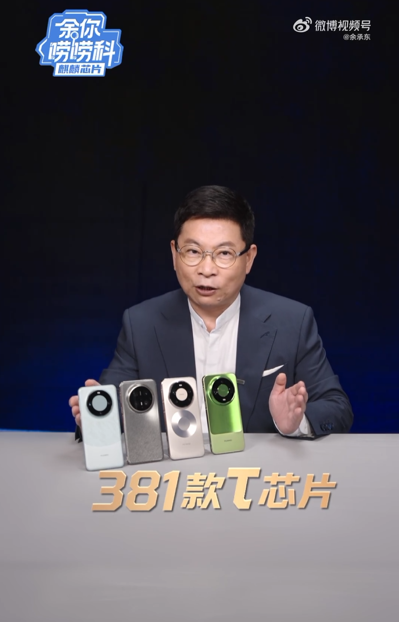 Figure: Technology roadmap and performance projection for Huawei Tau chips. Source: Huawei launch presentation.
Full-Stack Co-Design Compresses End-to-End Instruction Latency
Physical innovations in underlying hardware require tight software co-design to translate theoretical advantages into real-world performance gains. At the system level, Tau chips incorporate full-stack hardware-software-silicon co-optimization. In legacy compute architectures, instruction dispatch and execution flows are largely static and rigid. Under the Tau architecture, instruction streams and data pathways are dynamically scheduled in real time based on active device workloads.
This elevated control granularity enables the system to allocate constrained compute resources with far greater intelligence. Under heavy concurrent workloads, the silicon deploys deep instruction prefetching and high-accuracy branch prediction to amplify overall parallel throughput. System clock cycles are orchestrated with minimal dead time, drastically compressing end-to-end task turnaround latency. Complex compute routines that previously required several cycles to resolve can now deliver results in significantly condensed total durations.
Lingqu Bus Restructures Interconnect Memory Semantics Across Supernodes
No matter how capable an individual processor die may be, once scaled into massive compute clusters, inter-chip communication inevitably emerges as the primary system bottleneck. Frontier AI foundation model training and complex cloud inference routinely demand the synchronized coordination of hundreds or thousands of accelerator cards. To dismantle communication barriers across distributed nodes, Huawei defined its proprietary Lingqu Bus at the system architecture layer.
The Lingqu Bus overhauls the underlying interconnect protocols of high-performance computing clusters. It provides native support for unified memory addressing across hyper-scale compute nodes, breaking through conventional I/O throughput limits during inter-node data exchange. With native memory semantics, retrieving data across the network fabric feels as direct and low-overhead as addressing local physical memory. System-level communication latency is drastically slashed, transforming loosely coupled compute nodes into a tightly integrated supercomputing fabric and curtailing communication overhead penalties.
Targeting 1.4nm Equivalent Density by 2031
The semiconductor sector’s chronic anxiety over advanced process nodes largely stems from a path dependency on physical transistor density. Huawei’s engineering roadmap provides an alternative paradigm. According to official roadmaps, continued iteration along the Tau Law trajectory will allow high-end processors based on this architecture to achieve an effective transistor density on par with conventional 1.4nm nodes by 2031, accompanied by proportional gains in integrated computing capability.
The competitive landscape of silicon computing is expanding into new dimensions. Under external constraints that limit direct access to state-of-the-art lithography scanners, systemic engineering restructuring governed by time constants provides the most resilient technical path for domestic supply chains to bridge the node gap. This represents a compute trajectory anchored squarely in architectural efficiency.
381 Chips Assemble an Autonomous Multi-Terminal Hardware Foundation
The 381 Tau chips confirmed in the announcement do not represent an isolated prototype or a single product line. Their operational footprint spans core mobile SoCs for smartphones, high-performance autonomous driving platforms for intelligent vehicles, and hyperscale cloud AI acceleration clusters. This is a comprehensive silicon-level re-architecture originating from fundamental physical devices and expanding across the entire application ecosystem.
Executing an architectural transition of this magnitude demonstrates that Huawei has established an autonomous, full-scenario foundational compute substrate. Whether addressing the ultra-low latency demands of vehicle edge systems or the exacting power-efficiency constraints of consumer devices, sovereign hardware architectures provide the essential foundation. Moving beyond one-dimensional physical dimensional scaling, evolutionary pathways centered on temporal scaling are fundamentally redrawing the global computing competitive arena.
Reference Links:
- Video update on semiconductor business progress by Huawei Executive Director Richard Yu
- Huawei Keynote Address at the 2026 International Conference on Circuits and Systems