Deploying a 3-trillion-parameter model conventionally demands clusters of hundreds of high-end GPUs equipped with massive HBM pools. Frequent tensor-parallel synchronization across accelerators incurs heavy communication overhead, pinning generation throughput to a few dozen tokens per second. Cerebras took an entirely different architectural path: orchestrating 59 WSE-3T wafers to achieve throughput ranging from 1,000 to 2,000 tokens per second.
This deployment model departs from the standard assumption of fitting an entire model into a single shared memory pool. Engineers sliced the 93-layer network and permanently pinned weights across the on-chip SRAM of 59 wafer-scale engines. Inter-chip communication is stripped down to microsecond-scale activation passing. Accelerators are no longer passive memory containers; they have become physical assembly stations along a hardware pipeline.
93 Layers Sliced Across 59 Wafers: Pinning Weights Permanently On-Chip
The persistent bottleneck in frontier LLM inference has always been memory bandwidth. At 3 trillion parameters, even 4-bit quantized weights occupy 1.5 TB. In traditional GPU architectures, generating every single token requires streaming massive weight tensors from external DRAM into compute cores. This continuous memory transfer traps generation speeds behind the memory wall.
A single WSE-3T wafer integrates 44 GB of on-chip SRAM with an aggregate network-on-chip bandwidth reaching 53.5 PB/s. Kimi K3’s 93 layers average roughly 16 GB of weights per layer—fitting comfortably within a single wafer’s capacity. By loading and permanently locking layer weights directly into SRAM, engineers eliminated the costly round-trips to external memory entirely.
With weights static on-chip, the entire network stretches across a contiguous corridor of silicon. Each wafer executes only its designated layers, keeping compute cores tightly coupled to their local memory. Data streams along the physical hardware topology, directly mapping the model’s structural graph onto silicon.
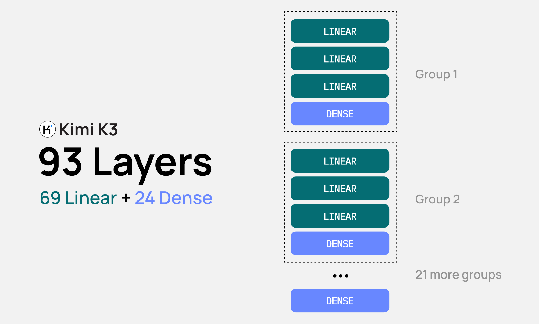 Figure: Kimi K3 layer architecture and wafer allocation breakdown. Source: Cerebras Blog
Decoupling Linear and Dense Layers: Byte-Level SRAM Budgeting
Kimi K3 adopts a hybrid architecture comprising 69 linear attention layers and 24 dense attention layers. Cerebras evaluated the deployment at an average context length of 256k tokens, using 4-bit weights and 8-bit KV caches. Because the two attention mechanisms present drastically different memory footprints, the wafer mapping required meticulous partitioning.
Linear attention layers maintain fixed-size hidden states during inference. Memory overhead remains strictly constant regardless of context expansion. Two linear layers combine for 32 GB of weights, leaving 12 GB on a single wafer for static state buffers. Consequently, all 69 linear attention layers are accommodated across just 35 wafers.
Dense attention layers, by contrast, absorb the full brunt of context scaling: a 256k sequence causes active requests to accumulate substantial key-value caches. To handle this demand, the team allocated an entire wafer per dense layer. Each wafer hosts 16 GB of weights, reserving the remaining 28 GB of SRAM exclusively for dynamic KV caches. The 24 dense layers consume 24 wafers, pairing with the 35 linear wafers to complete the 59-wafer cluster.
Passing Only Activations: 2-Microsecond Hops Complete the Pipeline
With weights fixed on-chip, inter-chip communication changes fundamentally. Conventional setups synchronize tensor slices across devices, where interconnect bandwidth dictates overall throughput. In the Cerebras pipeline, the network fabric carries only the intermediate activations produced by each layer’s forward pass.
The activation payload for a single forward step typically measures only a few megabytes. Within the CS-4 system architecture, each rack houses three wafers, compressing inter-wafer hop latency to just 2 microseconds. Activations traverse the network via RDMA over Ethernet, with 2-microsecond transfers introducing virtually zero pipeline stalls.
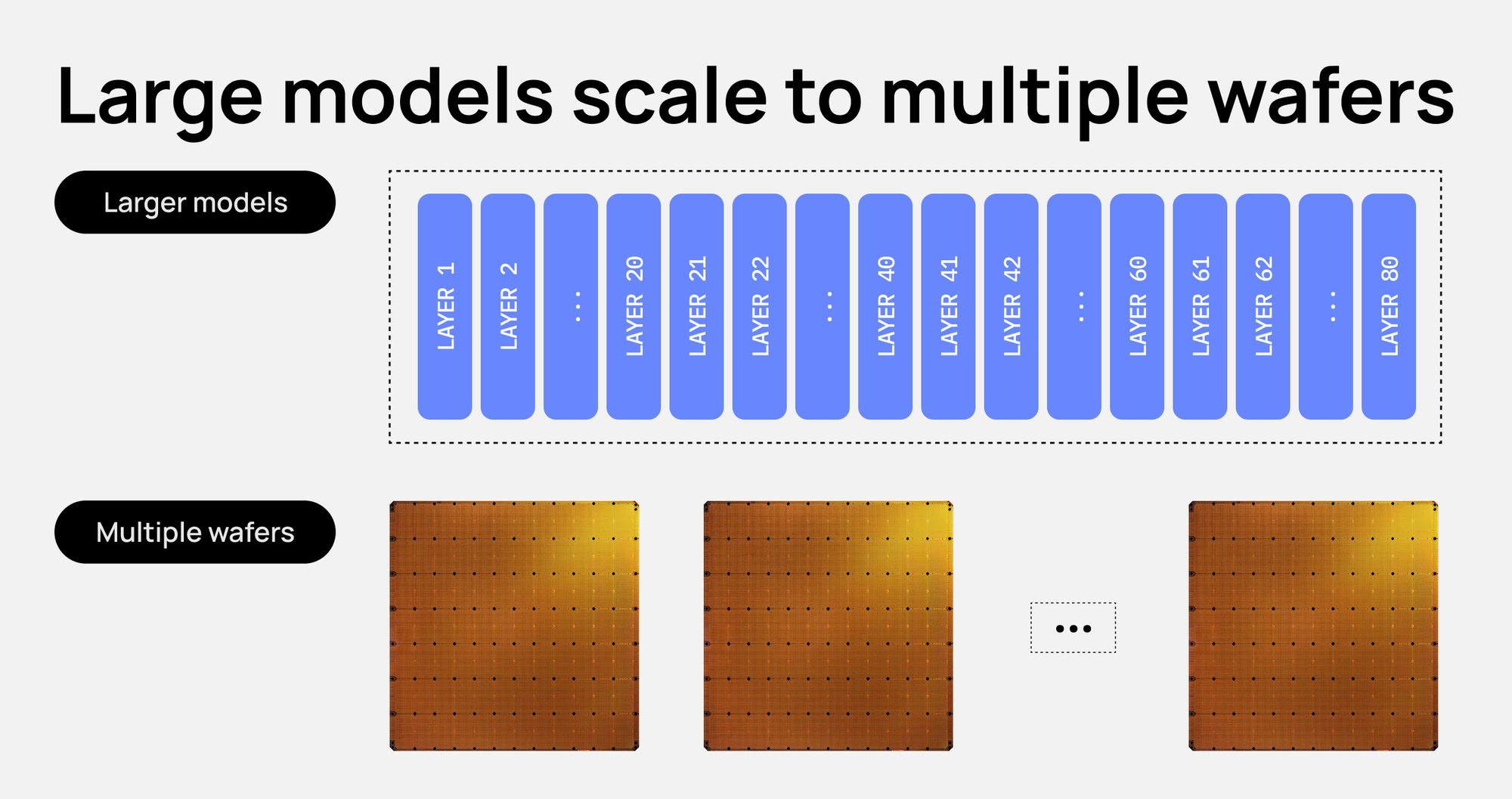 Figure: Communication topology across cascaded wafers, passing activations via RDMA over Ethernet. Source: Cerebras Blog
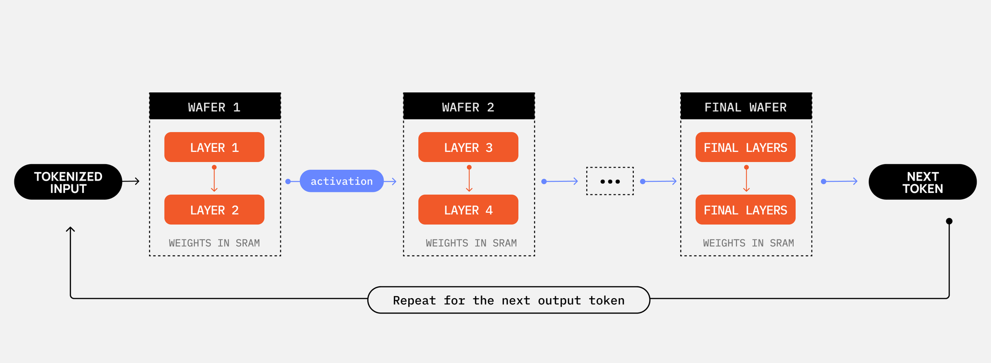 Figure: Assembly-line perspective of an individual request streaming across 59 wafer pipeline stages. Source: Cerebras Blog
The system functions much like an industrial assembly line. As soon as the first wafer finishes computing its layer, activations are dispatched to the downstream station. The upstream wafer is instantly freed to process the next incoming request. With 59 wafers executing concurrently, single-stream inference latency drops to the physical limits of the silicon.
Behind 2,000 Tokens/s: SRAM Capacity Defines the Concurrency Ceiling
Pipelining enables distinct stations to process independent requests simultaneously. While stage three computes for User A, stage two can execute a micro-batch for User B. Total concurrent in-flight requests roughly equal the number of pipeline stages multiplied by micro-batch size. Smaller batches minimize single-user latency, while larger batches maximize system-wide token throughput.
Yet blistering single-user generation speed comes with an uncompromising capacity constraint. Maximum system concurrency is bounded strictly by the on-chip SRAM across the 24 dense attention wafers. Every active request must secure dedicated KV cache space on each dense wafer, and 28 GB of available SRAM sets a hard ceiling on concurrent sessions.
Trading off-chip DRAM for on-chip SRAM unlocks thousands of tokens per second, but constrains concurrency elasticity. Traditional GPU clusters suffer from higher per-request latency but leverage massive memory pools to absorb tens of thousands of concurrent users. Once a wafer’s SRAM cache is exhausted, the hardware has no further headroom. Scaling concurrency requires deploying another complete 59-wafer pipeline.
Single-User Speed vs. Massive Concurrency: Two Diverging Hardware Paradigms
Kimi K3 achieved top-tier benchmark results: 88.3% on Terminal-Bench 2.1, rivaling GPT-5.6 Sol’s 88.8%, and 91.2% on BrowseComp, slightly surpassing Sol’s 90.4%. The evaluation demonstrates that frontier open-weight models deliver rigorous performance in complex agentic workflows.
This divergence is reshaping how industry measures inference efficiency. Historically, benchmarks prioritized raw concurrency and aggregate batch throughput. Cerebras argues the evaluation metric should shift toward tokens generated per megawatt at a guaranteed output latency. This lens measures how efficiently an architecture converts electrical power into interactive, real-time agent responsiveness.
The two hardware philosophies address fundamentally different commercial priorities. Agentic reflection loops require near-instantaneous output, where wafer-scale pipelining eliminates idle wait times. Conversely, for high-volume public APIs serving massive concurrent traffic, conventional GPU memory pools remain more economically elastic.
Running a 3-trillion-parameter frontier model across 59 wafers establishes a viable physical path through the memory wall. By redefining silicon from a passive storage container into an active assembly-line station, wafer pipelining resets the latency boundaries of modern LLM inference. The next phase of hardware competition will be decided by how seamlessly data flows across multidimensional physical topologies.
References:
- Cerebras Official Blog: How We Deploy Trillion-Parameter Frontier Models on Cerebras
- Kimi K3 Architecture and Benchmark Report
- Cerebras CS-4 System Architecture Whitepaper