Scores Surged by Nearly Half While Frequencies Stalled Near 5 GHz
2,016 points, 2,426 points, and 2,969 points: these are the single-core scores logged across three successive generations of AMD desktop processors on Geekbench 6. Comparing the Ryzen 7 5800X3D through the 9800X3D reveals an outcome that defies conventional intuition. Over the brief two-year span from 2022 to 2024, single-core performance within the same product tier jumped by 47 percent, while multi-core performance surged by 58 percent.
Decades of historical experience suggest that leaps of this magnitude must be powered by massive increases in clock frequency. But checking the specification sheets points in an entirely different direction. Moving from the Zen 3 architecture to Zen 5, the maximum boost clock inched up only from 4.5 GHz to 5.2 GHz, while base clocks rose from 3.4 GHz to 4.7 GHz.
A 15 percent frequency bump cannot bridge a performance gap of nearly 50 percent. Clock speeds stalled just past the 5 GHz barrier because heat dissipation and electrical leakage have slammed directly into physical limits. Pushing beyond 5 GHz demands non-linear voltage increases to preserve signal integrity; the resulting leakage current and concentrated thermal density can easily plunge silicon into a self-defeating thermal throttling loop.
These figures dismantle the traditional narrative: single-core performance gains no longer rely on higher clock frequencies. Since the processor’s assembly line cannot simply be clocked faster, chip architects had only one viable path forward—rebuild the pipeline from scratch and widen it to an unprecedented scale.
Widening the Lanes: Squeezing Five Billion Extra Transistors into the Core
With frequency scaling exhausted, widening microarchitectural structures horizontally became the only path to sustained performance growth. From Zen 3 to Zen 5, AMD consistently expanded the transistor budget of each chip. Total transistor counts climbed roughly 50 percent, swelling from approximately 11 billion to 16 billion.
Critically, those five billion additional transistors were not merely poured into massive cache arrays. Instead, they were channeled directly into core compute logic. In the instruction fetch and decode frontend, the most conspicuous change is dispatch width: Zen 3 could dispatch at most six instructions per clock cycle to the backend, whereas Zen 5 scales that up to eight.
Expanding decode and dispatch width from six to eight is vastly more complex than laying down extra wires. Because x86 instructions vary in byte length, decoders must predict boundaries and slice eight consecutive instructions in parallel without knowing where the preceding instruction terminates. Building that predictive machinery consumes immense die area and transistor budget on its own.
The integer execution backend saw an equivalent expansion. Earlier architectures relied on four integer arithmetic logic units (ALUs) to shoulder general-purpose computing workloads; Zen 5 raises that count to six. By processing significantly more basic operations during every cycle, the chip drastically increases pipeline execution throughput.
 Figure: An AMD Ryzen processor with its motherboard platform. Source: Wikimedia Commons, CC0
Swallowing 400 In-Flight Instructions: Doubling the Scheduler Lookahead
Adding wider execution pipelines is only half the battle; the real engineering feat lies in keeping those execution units continually fed. Modern high-performance processors rely heavily on out-of-order execution (OoO), dissecting forthcoming instruction streams to find independent work and calculating results ahead of time. This ability to anticipate instruction streams determines whether the newly added integer ALUs are firing at peak capacity or burning power while idling.
The core structure governing this predictive horizon is the Reorder Buffer (ROB). In Zen 3, the ROB held up to 256 instructions. When encountering branching code or high-latency main memory accesses, the scheduler’s limited lookahead window often failed to uncover enough independent instructions, forcing execution units to stall.
With Zen 5, AMD expanded the reorder buffer capacity to 448 entries. This cavernous structure allows the processor to hold nearly 500 instructions in flight simultaneously while running complex dependency analyses across them. The scheduler gains ample headroom to comb through tangled instruction streams and extract parallelizable computing tasks.
With an instruction window of this size, the chip no longer idles whenever a cache miss triggers a penalty of hundreds of cycles to retrieve data from system RAM. Instead, the scheduler scavenges through the 448-entry pool to locate independent workloads, keeping the execution pipelines continuously engaged throughout the wait.
| Processor Model | Architecture | Release Year | Single-Core Score | Max Boost Clock | Integer ALUs | Reorder Buffer Size |
|---|---|---|---|---|---|---|
| Ryzen 7 5800X3D | Zen 3 | 2022 | 2,016 pts | 4.5 GHz | 4 | 256 entries |
| Ryzen 7 7800X3D | Zen 4 | 2023 | 2,426 pts | 5.0 GHz | 4 | 320 entries |
| Ryzen 7 9800X3D | Zen 5 | 2024 | 2,969 pts | 5.2 GHz | 6 | 448 entries |
Doubling Data Paths: Ensuring Execution Units Never Wait for Cache
Scaling execution units and lookahead windows inevitably imposes punishing demands on the memory subsystem. If data cannot be ferried to execution units as fast as instructions are retired, wider pipelines quickly starve. Expanding cache hierarchies and broadening internal data buses become absolute imperatives to match frontend compute power.
The dedicated L1 data cache expanded from 32 KB to 48 KB, while the per-core private L2 cache doubled from 512 KB to 1 MB. Nestled right against the compute core, these ultra-low-latency memories ensure that frequent working data can be retrieved within a few clock cycles, drastically reducing how often the core must venture out to main memory.
For floating-point and vector workloads, AMD took an even more aggressive approach. Zen 3 and Zen 4 relied on four 256-bit SIMD execution units. Zen 5 replaces them with four full 512-bit units. Doubling vector width enables a single instruction to crunch sixteen 32-bit single-precision floating-point numbers simultaneously, providing immediate speedups for scientific simulation and local LLM inference.
To satisfy this high-throughput computational engine, memory load and store pathways were widened to match. The updated architecture sustains two 512-bit loads and one 512-bit store on every clock cycle. Massive bus bandwidth coupled with doubled cache tiers ensures data delivery matches the rapid pace of compute scaling.
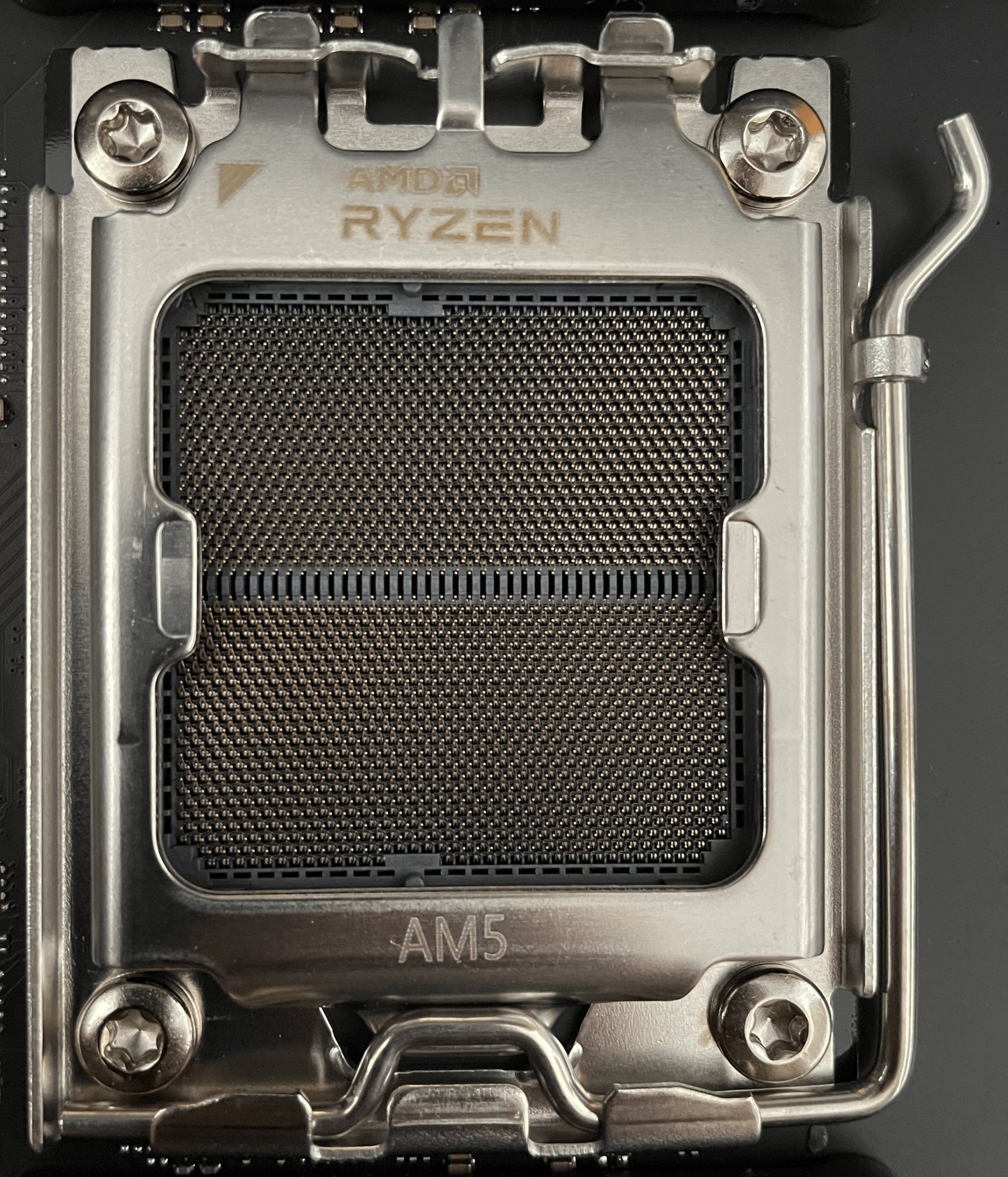 Figure: The AMD AM5 processor socket. Source: Wikimedia Commons, CC BY-SA 4.0
Trading Silicon Area for Speed: Who Bears the Thermal Bill?
Relying on sheer physical scale to extract performance incurs steep hardware costs. Adding five billion transistors means that even without chasing astronomical clock speeds, static leakage and active power consumption remain stubbornly elevated. Thermal density on the die is surging, and conventional air coolers find it increasingly difficult to tame these concentrated bursts of heat.
In practice, chip designers have offloaded the immense challenge of thermal dissipation—along with the cost of expansive silicon dies—onto motherboard power delivery networks and liquid cooling systems. More fundamentally, wider execution units and deeper instruction windows only translate into benchmark gains when software possesses exploitable parallelism. When code is inherently serial, these extra computing units sit idle while continuing to leak power and radiate heat.
For years, the rivalry between Intel and AMD revolved around a war of core counts. Yet simply tacking on more cores does not accelerate single-threaded latency. AMD’s choice to overhaul the core interior and widen microarchitectural throughput pushed the ceiling of single-core performance, breaking the industry habit of core-count inflation.
Talk of CPU stagnation misses the mark; progress has simply changed lanes. With clock speeds hitting diminishing returns, advancing single-core throughput requires exponentially larger and more intricate architectures. Early engineering leaks suggest that next-generation Zen 6 server chips are already targeting 256 cores and an astonishing 1 GB of L3 cache. On this path of widening architectures and packing in transistors, compute will keep marching forward—but every leap will demand increasingly formidable cooling gear and heavier power bills from users.
Reference Links:
- How did AMD Ryzen get 50% faster in two years?
- HN Discussion (item?id=49758709)